
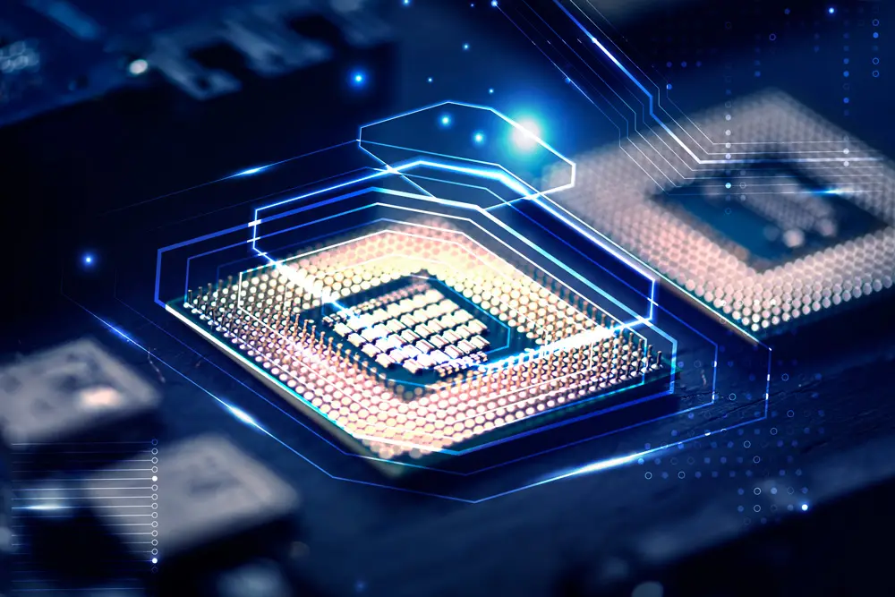
Industry-Focused Semiconductor Learning
Intelligent Chip Labs offers specialized training programs covering the key domains of modern chip design. From digital architecture and verification to physical design and test methodologies, students gain exposure to the complete semiconductor development flow.
Advanced Digital Design & VLSI Design
This course focuses on advanced digital design techniques used in modern semiconductor development. Students learn how to design high-quality RTL architectures, understand low-power design strategies, and explore AI-assisted design methodologies.
Key Learning Areas
- CMOS logic and digital design fundamentals
- Advanced RTL architecture and FSM design
- Multi-clock and CDC-aware design techniques
- Low-power chip design strategies
- AI-assisted RTL analysis and optimization
- Timing closure and RTL-to-GDS flow

Frontend Design & Verification
Verification plays a critical role in ensuring that semiconductor designs function correctly before fabrication. This course introduces industry-standard verification methodologies and modern SystemVerilog-based verification environments.
Key Learning Areas
- SoC frontend lifecycle and verification planning
- SystemVerilog testbench development
- Assertion-based verification
- UVM methodology and architecture
- AI-driven verification analytics and debugging
- Coverage analysis and verification sign-off
Design for Test (DFT) & Performance Verification
Testing is essential to ensure semiconductor chips operate reliably after manufacturing. This course introduces DFT architecture, test coverage methodologies, and modern approaches to performance verification.
Key Learning Areas
- Fault models and manufacturing defect analysis
- Scan-based DFT architecture
- ATPG flow and coverage metrics
- Memory and logic BIST techniques
- AI-driven test pattern generation
- Performance analytics and predictive failure analysis


Physical Design
Physical design converts digital logic into a manufacturable silicon layout. This course introduces the complete physical implementation flow used in semiconductor companies.
Key Learning Areas
- RTL-to-GDS physical design flow
- Floorplanning and power planning strategies
- Placement and congestion optimization
- Clock tree synthesis and timing optimization
- AI-driven placement and routing techniques
- Physical verification and tape-out readiness
How to Join the Program
Intelligent Chip Labs offers specialized training programs covering the key domains of modern chip design. From digital architecture and verification to physical design and test methodologies, students gain exposure to the complete semiconductor development flow.
Submit Application
Counseling Session
Admission Confirmation
Start Training